Pattern Transfer Using The Etching Technique
- The layer is first blanket deposited; then the
patterned resist is formed and the layer is etched using the resist as a
mask.
- If the etching process attacks the layer
surface equally in all directions, the etch is said to be isotropic.
- For feature line widths and line spaces
significantly larger than the feature height, isotropic etching presents
only a minor problem.
- For VLSI devices, in which feature heights
have comparable dimensions to feature line widths and spaces, mask
compensation to account for isotropic etching is impossible. For this
reason plasma etch techniques, which are capable of anisotropic etching,
are so important to VLSI. [5]
- The degree of anisotropy of an etch process
can be expressed as
A = 1 – Vh/Vv
Where A
is the degree of anisotropy, Vh is the horizontal etch rate and Vv
is the vertical etch rate. [2]
- Isotropic etching is represented by A=0 and
anisotropic etching by A=1. [2]
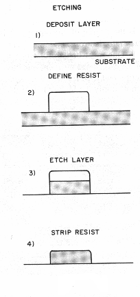
Fig. 5 Shows the
deposit/resist/etch/strip sequence of etching. [2]