Furnace Annealing
The electrical behavior after
implantation is dominated by deep-level electrons and hole-traps, which capture
carriers and make resistivity high. Annealing
is heating the wafer at high temperature for a specific time to repair lattice
damage and to move dopant atoms on substitutional sites where they will be
electrically active.
The success of the annealing is
measured in terms of the fraction of the dopant atoms that will become
electrically active.
Also the aim is to keep shallow
implants shallow by minimizing diffusion.
Furnace annealing has times on the order of minutes.
Annealing depends on dopant type, dose and whether the silicon has been made
completely amorphous or if it is partially disordered.
For amorphous silicon, regrowth
is by solid phase epitaxy. The amorphous/crystalline interface moves towards
the surface at a fixed velocity that depends on temperature, doping and crystal
orientation. Activation energy for SPE is 2.3 eV indicating that the process
involves bond breaking at the interface. Impurities such as B,P, As increase
the regrowth because they increase the number of broken bonds.[2]
If the silicon is partially
amorphous then lattice repair occurs by the generation and diffusion of point
defects. This process has an activation energy of about 5eV and requires
temperatures on the order of 900°C to
remove all defects.
Isochronal annealing plots,
showing the fraction of activated dopant as a function of temperature for a
fixed annealing time can summarize annealing characteristics.[1]
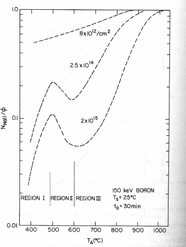
Fig. 8 Isochronal annealing of
boron. The fraction of activated dopant is plotted against anneal temperature
for different implant doses.[2]
|
Region I |
Region II |
Region III |
|
Below 500°C point defects dominate free
carrier concentration. As temperature increases these defects diffuse and
combine. Net carrier concentration increases as many traps anneal out. |
Above 500°C extended defects are formed
which reduce the number of substitutional boron atoms and cause a net
decrease in carrier concentration. This is called Reverse Annealing. |
Above 600°C fraction of activated dopant
atoms increases as point defect generation and migration allows precipitates
and dislocations to dissolve. |