Silicon
Shaping
As
silicon is a hard, brittle material, the most suitable materials for shaping
and cutting silicon are the following.
·
Industrial-grade
diamonds
·
SiC and Al2O3
Shaping
Operations involves the following:
·
Removing the seed and
tang ends from the ingots
·
Surface grinding
which defines the diameter of the material.
·
After diameter
grinding one or more flats are ground along the length of the ingot. The larger
flat is called "primary" flat. Purpose of primary flat (a) it is used
as a mechanical locator in automated processing equipment to position the
wafer. (b) Serves to orient the IC device relative to the crystal. Other
smaller flats are called "secondary" flats. Purposes of secondary
flat (a) identify the orientation and conductivity type of the material. (b)
Provide a means of quickly sorting and identifying wafers should mixing occur.
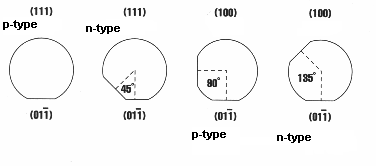
Fig. 9 Standard flat orientations for
different semiconductor wafers [4]
After
removal of seed and tang ends from the ingot, surface grinding and grounding
flats the ingot is ready to be sliced into wafers.
Slicing
determines four wafer parameters:
·
surface orientation
·
thickness
·
taper
·
bow
Polishing is the last step and it
is done to obtain a smooth, specular surface on which device features can be
photoengraved [2]. The aim is to produce a surface with a high degree of
surface flatness and minimum local slope to meet the requirements of optical
projection lithography. Typical values of surface flatness are between 5 and 10
microns. In the chemical mechanical polishing (CMP) process, the wafer is held
on a rotating holder and pressed on a rotating polishing pad, with slurry and
water in between. The slurry is a colloidal suspension of fine silica particles
with diameters of about 100°A in an aqueous solution of sodium hydroxide [3]. Sodium hydroxide
oxidizes the silicon surface (chemical process) with the help of heat generated
by the friction between the wafer and polishing pad. Then the silica particles
abrade the silicon oxide away from the surface (mechanical process). Figure [2]
below gives a schematic of the CMP process.
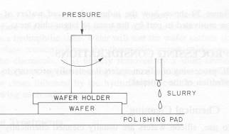
A schematic of CMP process[2].