Crystal
Pulling
EGS
is placed in a rotating quartz crucible and melted at 1415ºC. A rotating seed
crystal is slowly punched into the molten silicon, then slowly pulled out to
obtain an ultra-pure, single-crystal silicon ingot. Single-crystal silicon wafers
are obtained by sawing the round ingot into slices. Then wafers are lapped,
cleaned, etched, polished, labeled, and shipped to IC chip manufacturers.
There
are two methods commonly used in the semiconductor industry to generate
single-crystal silicon, the Czochralski (CZ) method and the floating zone (FZ)
method. The CZ method is cheaper and can produce larger size wafers whereas the
FZ method can produce wafers with high purity.
CZ Method
·
The majority of
silicon wafers used in IC processing are made from the CZ method (Fig. 7). The
process takes place in a sealed chamber with argon ambient to control
contamination.
·
In the CZ method, the
high-purity EGS is melted in a slowly rotating quartz crucible at 1415ºC, just
above the silicon melting point of 1414ºC, by radio frequency (RF) or resistive
heating coils.
·
A single-crystal
silicon seed rod mounted on a slowly rotating chuck is gradually lowered into
the molten silicon, and the surface of the seed crystal submerges in the molten
silicon and starts to melt.
·
The seed crystal
temperature is precisely controlled at just below the silicon melting point.
When system reaches thermal stability, the seed crystal is withdrawn very
slowly, dragging some molten silicon to recondense around it with the same crystal
orientation.
·
The ingot, a whole
piece of single-crystal silicon is formed after up to 48 hours of pulling.
·
The diameter of the
crystal in the CZ method can be controlled by the temperature and pulling rate.
·
Single-crystal
silicon ingots pulled by the CZ method have trace impurities of oxygen and
carbon, which come from the crucible materials.
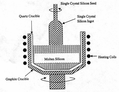
Fig.
7 Schematic of the Czochralski (CZ) crystal-pulling method [3]