Line Defect/Dislocation
·
Two general
categories of dislocations are screw
and line. Fig. 6 shows a schematic
representation of a line distortion in a cubic lattice; it can be seen as an
extra plane of atoms AB inserted into the lattice.
·
Dislocations in a
lattice are dynamic defects; that is, they can move under applied stress,
dissociate into two or more dislocations, or combine with other dislocations.
·
Crystals to be used
in IC fabrication are generally grown free of edge dislocations, but may
contain small dislocation loops from excess point defect condensation. These
defects act as nuclei for the precipitation of impurities such as oxygen and
are responsible for a swirl pattern seen in wafers.
·
Dislocations in
devices are generally undesirable, because they act as sinks for metallic
impurities and alter diffusion profiles.
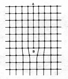
Fig. 6 An edge dislocation in a cubic lattice
created by an extra plane of atoms. The line of the dislocation is
perpendicular to the page. [2]